


For more efficient power management in system-on-chips (SoCs), a fully integrated voltage regulator (FIVR) running at a high switching frequency would be an ideal solution to supply an optimized point-of-load (PoL) voltage with a rapid dynamic voltage scaling (DVS) capability. Additionally, because high throughput performance is required even in mobile SoCs, a multi-phase (MP) architecture with many inductors has become essential in FIVRs for efficiently powering heavy load.
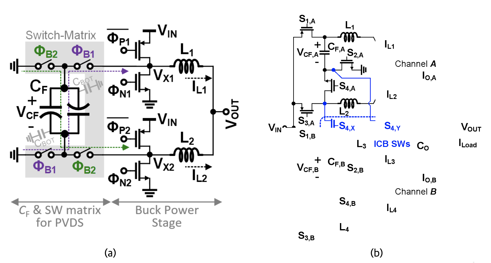
In practical use, MP-FIVRs suffer from an inter-inductor current imbalance. Specifically, because of the tight on-chip area constraint, multiple integrated inductors must be closely spaced, thereby aggravating parasitic inductive coupling (PIC) effects. This article introduces a new current-balancing scheme based on a flying-capacitor, which can equalize inductor currents at the true-average. The proposed PVDS (Fig 1. (a)) benefits highly balanced inductor currents owing to fully-differentially and directly detecting ∆IL via the flying-capacitor (CF) in addition to a minimum power overhead of 2.1 mW, which occupies only 1 ~ 1.4% of total power loss at ILoad = 1.5 A. Furthermore, by combining it with the dynamic reallocation of on-chip capacitors, the PVDS consumes a minimum chip area without sacrificing the power density. Also, the proposed 2L1C (Fig 1. (b)) can self-correct the current imbalance between the inductors only by a flying-capacitor with no extra overhead. Compared to the multi-phase & multi-level (MPML) converter, the number of flying-capacitors and power switches in the proposed design can also be decreased two-fold while inheriting the ML converter’s benefit of a lower switching voltage ∆VX (= VIN/2) enabled by CF, thereby bringing an improved power density and efficiency.
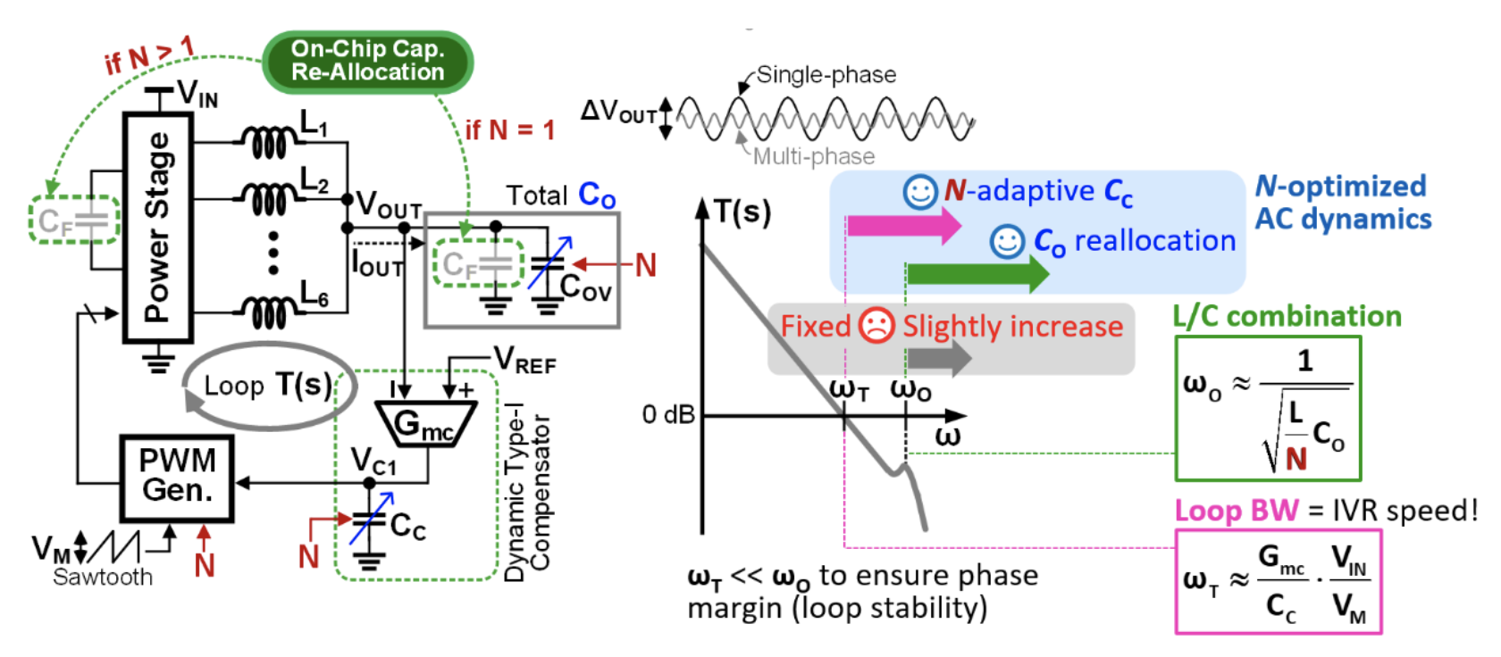
Another key idea is to reallocate on-chip capacitors adaptively to the number of phases and reuse the surplus CO as a flying-capacitor CF utilized in the PVDS. As N approaches its maximum (Nmax = 6), the total CO is reduced further by lowering COV. As a result, ωO moves to a much higher frequency as N increases. The capacitor CC of the dynamic type-I compensator is designed to be changed in accordance with N. This enables ωT to closely track the extremely moving ωO while maintaining a certain margin (ωT < 6×ωO).
This article is based on research published in the the IEEE Journal of Solid-State Circuits 2022 and IEEE Journal of Solid-State Circuits 2024.
Jeong-hyun Cho School of Electrical Engineering, KAIST
E-mail: jh-cho@kaist.ac.kr
Homepage: https://www.icdesignlab.net
