


The main goals of PIM-SDRC are to build an ecosystem to connect industry-academia-research institutes for PIM development via the three activities displayed in Figure 1.
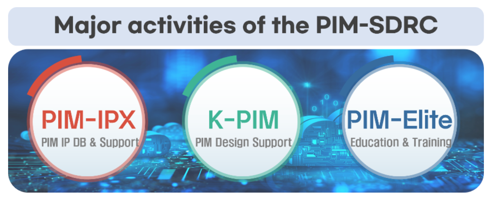
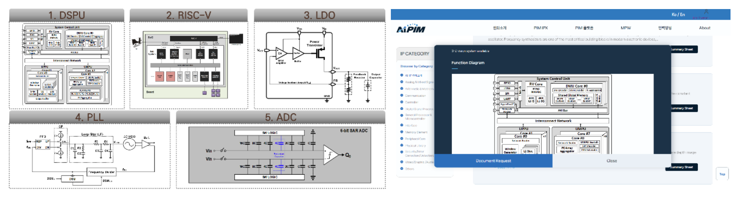
[PIM-IPX] Database(DB) center of PIM semiconductor IPs.
PIM-SDRC plays the role of PIM IP Hub by collecting, choosing, and managing competent PIM design IPs in a way that will eventually provide IPs as an open source, so that circuit designers can freely utilize verified IPs for PIM product development. To this end, PIM-SDRC has installed a high-performance server farm to make a large amounts of data handling possible for database processing of PIM products and IPs. It also opened a website to allow free access of PIM IPs and exchange of technical information among PIM researchers.
[K-PIM] PIM development infrastructures
PIM-SDRC is building research infrastructure for semiconductor PIM IPs in collaboration with universities, research institutes, and industries. The steering committee consists of a limited number of experts from Samsung, SK Hynix, and universities in Korea. PIM-SDRC is making its best efforts to provide MPW (Multi Project Wafer) services to the universities involved in the project and to form SIG (Special Interest Group) including EDA, design houses, and ventures, etc., to assist relevant stakeholders in developing and extending their businesses in the PIM area.
[PIM-Elite] Training
In 2022, the center provided special lectures on recent trends in PIM design technologies to more than 400 undergraduate and graduate students from about 20 universities across the country. From the enthusiastic atmosphere in the lectures, we came to realize how popular and interesting PIM is to students. PIM-SDRC also signed an agreement on PIM design research and training with Samsung, laying the cornerstone for PIM cooperation with the main industrial sites. PIM-SDRC designs short and mid-term programs to intensify manpower training in this arena.
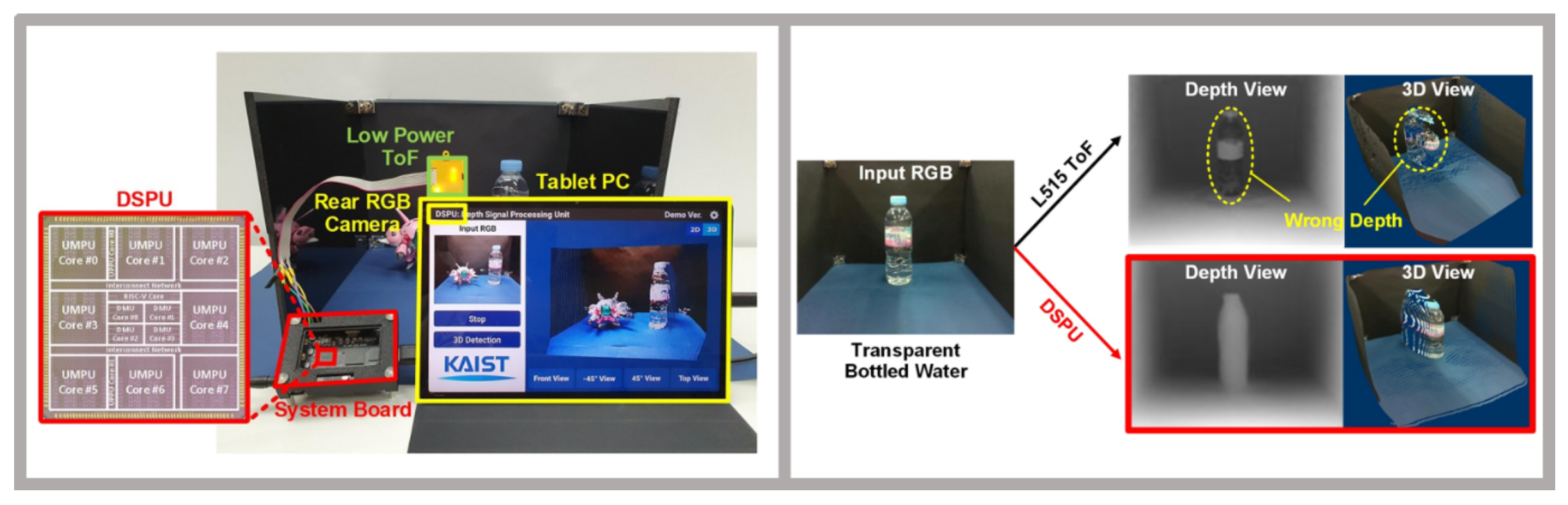
As of the end of the year 2022, PIM-SDRC was successful in developing an AI chip that is able to extract three-dimensional pictures from two-dimensional photo images by using deep neural network (DNN) inference and sensor fusion techniques. This is the first event of its kind using SRAM PIM IPs. Recently, it also successfully developed high-density and high-efficiency analog DRAM PIM based on triple-mode cells; this is believed to be another advanced step toward PIM IP development.
Prof. Hoi Jun Yoo
Dept. of Electrical Engineering, KAIST
KAIST Institute for IT Convergence
E-mail: from541@kaist.ac.kr
Homepage: http://itc.kaist.ac.kr, https://ai-pim.org/pim-ipx/intro/
