A way to transfer graphene
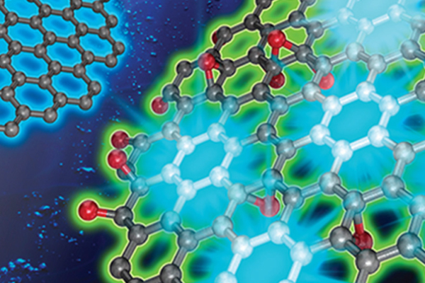
Since Andre Geim and Konstantin Novoselov at the University of Manchester discovered how to isolate a single atomic layer of carbon atoms from graphite by using Scotch tape in 2004, this new material called “graphene” became explosively popular in scientific communities because of its intriguing properties such as outstanding thermal/electrical conductivity, excellent mechanical strength, and high flexibility. Particularly, intense efforts are under way to utilize graphene in electronic applications as graphene is considered to be a promising candidate as a flexible and transparent electrode and a new gateway material in field-effect transistors (FETs). One of the key technologies to be developed for these applications is a transfer technique that can deliver graphene of a high purity level to a desired substrate over a large area without defects. Currently, graphene is grown on copper using chemical vapor deposition (CVD) that includes the deposition of vaporized carbon atoms at a very high temperature (~1000 °C). Then copper is etched with a chemical solution to float the graphene which is picked up by a target substrate (“fishing”). However, contamination usually occurs during this “wet transfer” process as ionic impurities or metallic residues are also transferred with the graphene and trapped at the interface between the transferred graphene and the target substrate. This contamination issue has been of great concern particularly for electronic applications where contamination ruins the electrical properties of the graphene devices and reduces their reliability.
Stamping with graphene
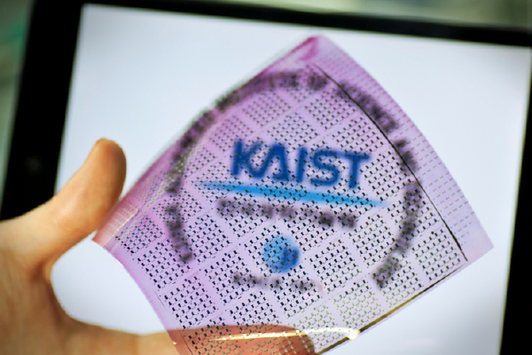
Recently researchers at KAIST, led by Professor Sung-Yool Choi in the Department of Electrical Engineering and the Graphene Research Center at the KAIST Institute, developed a new transfer technique that does not involve the metal etching step in the process. Their idea was simple: they thought of graphene on copper as “ink” which can be picked up with a “stamp” and transferred onto a new substrate by “stamping” it. With this new stamping technique, the team was able to transfer graphene without contamination so they could fabricate a graphene transistor with improved performance. They even succeeded in multiple stamping to produce multilayer graphene and also demonstrated large-area transfer of graphene onto various substrates including a flexible substrate and a structured electrode surface. Their report on this method was published in Small on January 14, 2015 and highlighted on the front cover of the issue. This new technology was also featured on Arirang TV and the video clip can be found at the following link: (https://www.youtube.com/watch?v=-6C0pLG3c9g).
Poly (vinyl alcohol): the secret ingredient
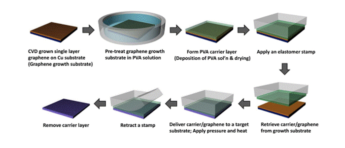
The biggest challenge for the team was to develop a method to delaminate the graphene from the copper when the graphene is in contact with the stamp. “Eliminating the metal etching step was the best way to overcome all of the issues related to the conventional transfer method. But that meant we had to find another way to separate the graphene from the copper,” said Dr. Sang-Yoon Yang, a research professor in Choi’s group who is the first author of the paper. The team found that the graphene could be readily detached from the copper surface when they treated graphene grown on copper with an aqueous solution of poly (vinyl alcohol) (PVA) and then, deposited the PVA carrier layer on the treated graphene surface. Use of the PVA is the real key in this process because it mediates the interaction between the graphene and the stamp. This polymer, consisting of a hydrocarbon backbone and a number of pendent hydroxyl groups, is spontaneously adsorbed onto the hydrophobic graphene surface during the treatment step in the PVA solution, which enables the enhanced interaction between graphene and the PVA carrier layer. After conformal contact is established between the elastomeric stamp and the carrier layer, quickly lifting the stamp up provides the maximized adhesion force between the stamp and the carrier layer, resulting in the delamination of the graphene from the copper surface. The only remaining work to do is pressing the “inked” stamp onto any target substrate to transfer the graphene. In this case, slowly releasing the stamp at a high temperature (130°C) creates defectless transfer of the graphene as the adhesion force between the elastomeric stamp and the carrier layer becomes weak under this condition. The substrate onto which the graphene is transferred is now ready for use after simply washing out the carrier layer with water (since PVA is water-soluble). The graphene is not contaminated with ionic or metallic impurities during the transfer process so the quality is sufficient to be used for device fabrication. Indeed, the team fabricated a graphene FET using this technique and proved that the FET showed improved performance due to the absence of interfacial impurities.
More can be done with stamping
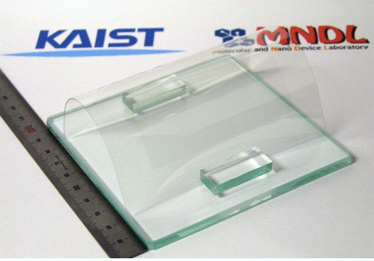
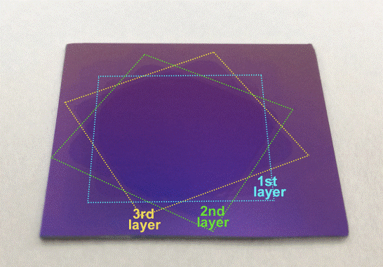
“Our method is very eco-friendly and cost effective because we do not use hazardous metal-etching chemicals, unlike the wet transfer method, and we can reuse the copper substrate and grow the graphene on it multiple times. Also, stamping is easier for transferring graphene over a large area than fishing for the floating graphene in the wet transfer process. These features will be good news to the electronics industry from the standpoint of mass productivity of graphene-coated substrates,” said Professor Choi, who led the research team. To further prove the versatility of this technique, the team demonstrated that wafer-scale graphene up to four inches can be stamped (with the carrier layer) onto a variety of substrates, including a flexible substrate such as poly (ether sulfone) and a structured electrode surface. Even multilayer graphene, with a controlled number of layers, can be formed on a substrate simply by stamping it multiple times. Now the team is exploring ways to apply this technique to other emerging two-dimensional (2D) materials beyond graphene. They expect that the effective combination of graphene with other 2D materials based on this technique will pave the way towards the realization of nano-scale electronic devices with unconventional operating principles.
This work was supported by the Global Frontier Research Center for Advanced Soft Electronics (2011-0031640, 2011-0031660 and 2011-0031638), the Nano-Material Technology Development Program (2012M3A7B4049807), and the Basic Research Program of ETRI (13ZE1110).


