Organic insulator: a key material for future soft electronics
A field-effect transistor (FET) is an essential component of modern electronic devices from cell phones and computers to flat-panel displays. A FET consists of three electrodes (gate, source, and drain) fabricated on a semiconducting substrate where the gate electrode is separated from the semiconductor by a thin layer of insulating material. The insulating layer enables the current to be controlled between the source and the drain electrodes by bias voltage applied at the gate electrode.
While inorganic oxides and nitrides have been used as insulating materials for conventional FETs built on a hard surface such as silicon, the emergence of soft electronics now requires the use of organic insulators which are flexible and, at the same time, electrically robust and ultrathin in order to make the reliable and low-power operation of FETs possible. However, the fabrication of such organic insulating layers has been challenging due to difficulties in the formation of ultrathin films without pinhole defects over a large area.
Initiated chemical vapor deposition (iCVD) for the fabrication of an ultrathin polymer insulating layer
A research team at KAIST led by Professor Sung Gap Im in the Department of Chemical and Biomolecular Engineering and Professor Seunghyup Yoo in the Department of Electrical Engineering recently developed a route to synthesize ultrathin polymeric insulators by using an initiated chemical vapor deposition (iCVD) process. The research was published in Nature Materials (http://www.nature.com/nmat/journal/v14/n6/full/nmat4237.html) June 2015.
Compared with the conventional technique for the fabrication of polymer thin films that involves the spin coating of a polymer solution on a surface and the subsequent evaporation of the solvent, the iCVD process is quite unique as it is a solvent-free, vapor-phase deposition process. The iCVD process begins with a monomer and an initiator, not a polymer. The monomer and the initiator are vaporized and introduced in a chamber where a substrate is placed, and a polymer thin film forms via free-radical polymerization of the adsorbed monomer on the substrate surface keeping conformal contact with the surface. Owing to the surface-growing characteristics of iCVD, the process can overcome problems associated with surface tension to produce highly uniform, pure, and ultrathin polymer films over a large area with virtually no surface or substrate limitation. As no solvent is used and the substrate temperature is usually near room temperature, damage and stress to the substrate are minimized during the process.
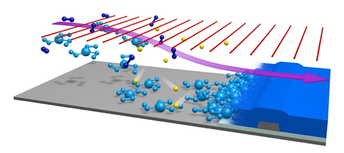
In particular, the authors investigated iCVD of 1,3,5-trimethyl-1,3,5-trivinyl cyclotrisiloxane (V3D3), a silicon-containing cyclic molecule with three polymerizable vinyl groups, for the fabrication of polymer insulating layers. Using iCVD, V3D3 formed a densely crosslinked and amorphous polymer film (pV3D3) with excellent insulating properties comparable to conventional inorganics even when the thickness was less than 10 nm. The pV3D3 layer also exhibited remarkable flexibility up to 4% of tensile strain when the layer was fabricated on poly(ethylene terephthalate), a well-known flexible and transparent polymer, indicating the superior flexibility of the pV3D3 layer to that of the inorganic counterparts.

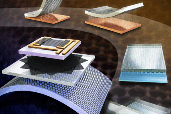
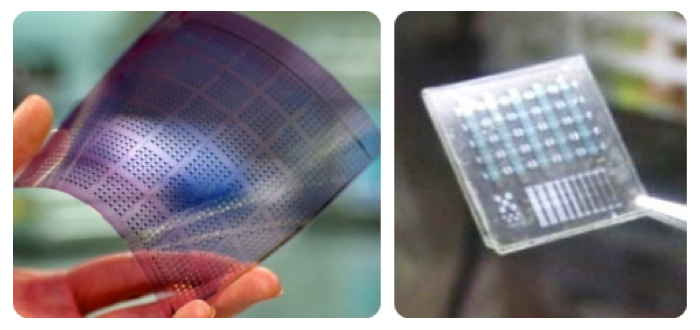
In collaboration with Professor Byung Jin Cho in the Department of Electrical Engineering at KAIST, the research team was able to build low-power and high-performance FETs containing pV3D3 film as the insulator. The wide range of material compatibility of pV3D3 allowed the team to manufacture FETs and electronic devices with various gate electrodes and semiconductors including oxides, graphene, and organics. Fabricating FETs on a flexible substrate was straightforward, and they demonstrated it with a FET array containing poly(3-hexylthiophene) as the semiconductor and pV3D3 as the insulator on 10 × 10 cm2 of poly(ethylene naphthalate). It was even possible to fabricate a stick-on, removable electronic component using conventional packaging tape as a substrate.
Promise in future electronic devices
The damage-free and conformal nature of the iCVD process is a key component in the formation of ultrathin films with ideal insulating properties. Professor Im noted, “The down-scalability and wide range of compatibilities observed with iCVD-grown pV3D3 are unprecedented for polymeric insulators.” He expects this technology to greatly benefit developing low-power and high-performance soft electronics which will be crucial for the success of emerging electronic devices such as wearable computers.
This work was supported in part by the Basic Science Research Program through the National Research Foundation of Korea (NRF) funded by the Ministry of Science, ICT and Future Planning (MSIP) (Grant Nos 2011-0010730 (S.G.I.), 2013-065553 (B.J.C.), NRF-2014R1A2A1A11052860 (S.Y.)), and by a grant from the Center for Advanced Soft Electronics funded by the MSIP as a Global Frontier Project (Grant Nos CASE-2011-0031638 (B.J.C.), CASE-2014M3A6A5060948 (S.Y.), CASE-2013M3A6A5073183 (Y-Y.N.)).


